How to Pass EMI/EMC Testing on the First Attempt
EMI/EMC testing failures are among the most expensive problems in product development. Each failed test costs $5,000-20,000 in lab fees plus weeks of delay. This guide provides practical strategies to maximize your chances of passing EMC testing on the first attempt, based on our experience helping dozens of power electronics products achieve compliance.
Understanding EMC Requirements
Before designing for EMC, you need to understand what standards apply to your product.
Common Standards:
For Power Electronics:
- FCC Part 15: US radiated and conducted emissions
- CISPR 11/32: International emissions (IEC 61000-4 series)
- EN 55032: EU emissions
- EN 55035: EU immunity
- IEC 61000-4-x: Immunity tests (ESD, surge, fast transient, etc.)
Emission Limits:
Class A (Industrial): Less stringent, 10dB higher limits
- Radiated: 30-40 dBμV/m at 10m
- Conducted: 79-73 dBμV (150kHz-500kHz), 73-60 dBμV (500kHz-30MHz)
Class B (Residential): More stringent
- Radiated: 30-37 dBμV/m at 10m
- Conducted: 66-56 dBμV (150kHz-500kHz), 56-46 dBμV (500kHz-30MHz)
Frequency Ranges of Concern:
- 150kHz - 30MHz: Conducted emissions (measured on power lines)
- 30MHz - 1GHz: Radiated emissions (measured in shielded room)
-
1GHz: Increasingly important for high-speed digital interfaces
Key Insight: Most power electronics failures occur in the conducted emissions range (150kHz-30MHz) due to switching frequency harmonics.
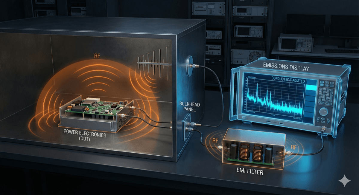
Pre-Compliance Testing Strategy
Pre-compliance testing in your own lab or at a lower-cost facility can catch problems before expensive formal testing.
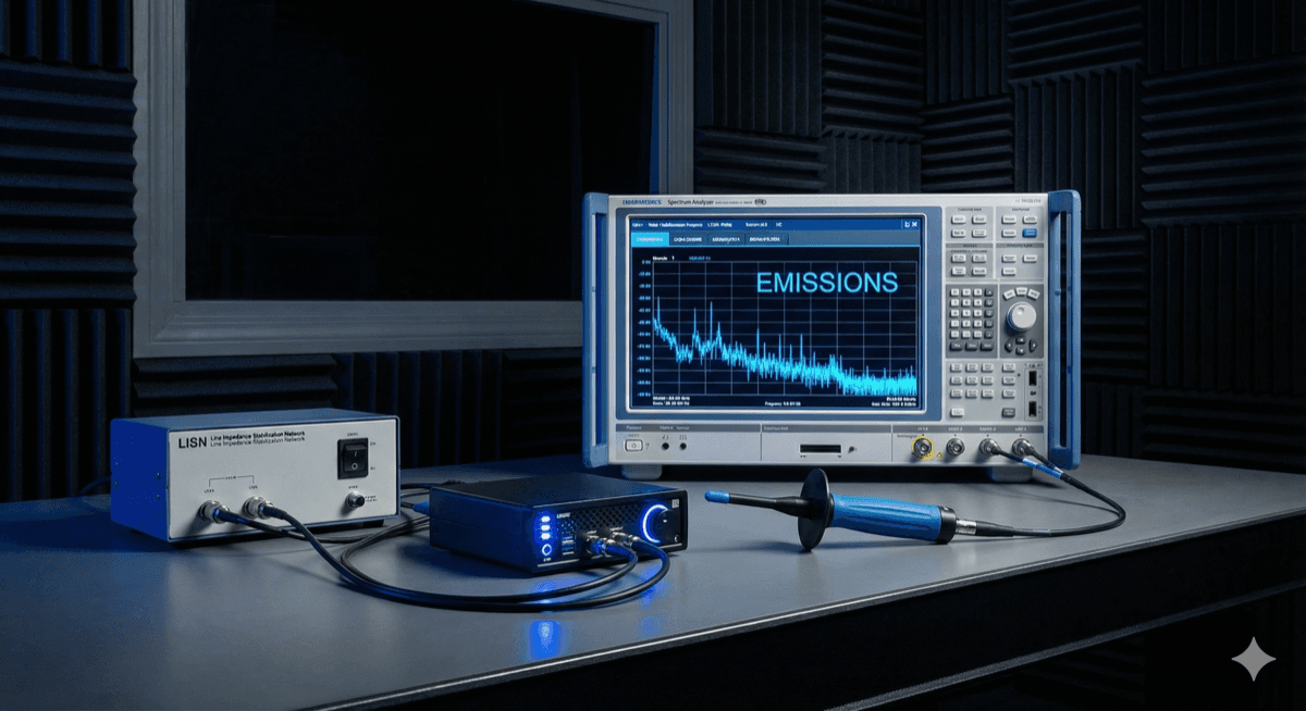
Essential Pre-Compliance Equipment:
-
Spectrum Analyzer: $2,000-20,000
- Minimum: 9kHz-3GHz range
- EMI receiver mode preferred
- Peak/quasi-peak/average detectors
-
LISN (Line Impedance Stabilization Network): $500-2,000
- Provides standard 50Ω/50μH impedance
- Separates DUT from power source
- Required for conducted emissions
-
Near-Field Probes: $200-1,000
- H-field (magnetic) probes for current loops
- E-field probes for voltage nodes
- Essential for locating emission sources
-
Shielded Room or Open Area: Variable cost
- Basic shielded enclosure for conducted: $5,000-20,000
- Full anechoic chamber for radiated: $100,000+
- Alternative: Outdoor open area test site
Pre-Compliance Process:
-
Conducted Emissions First:
- Easiest to measure and fix
- Use LISN and spectrum analyzer
- Compare to applicable limits
- Document frequency and amplitude of peaks
-
Near-Field Scanning:
- Probe around the unit with H-field and E-field probes
- Identify locations of maximum emissions
- Correlate frequencies with switching harmonics
- This guides where to add filtering/shielding
-
Radiated Emissions:
- Requires larger test setup
- Can use nearby EMC lab for single pre-scan
- Focus on peaks identified in near-field scanning
Cost/Benefit: $5,000-10,000 in pre-compliance testing can prevent $20,000-50,000 in failed formal tests and redesign costs.
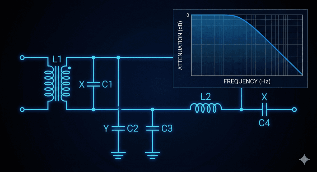
EMI Filter Design
Proper EMI filter design is the most effective way to address conducted emissions.
Filter Topology:
A typical power electronics EMI filter includes:
-
Common Mode Choke:
- Addresses noise that flows equally on both power lines
- High impedance to CM noise, low impedance to differential power
- Typical values: 1-10mH for 50/60Hz applications
-
Differential Mode Filter:
- Addresses noise between power lines
- Typically: Series inductors + X-capacitors
- Values: 10μH-1mH inductors, 0.1-1μF X-caps
-
Y-Capacitors:
- Connect line to ground/chassis
- Limited by safety leakage current requirements
- Typical: 1-4.7nF per line (Class Y2)
Design Process:
-
Measure Unfiltered Emissions:
- Identify peak frequencies and amplitudes
- Calculate required attenuation to meet limits (with margin)
-
Calculate Filter Corner Frequency:
- fc = peak frequency / (required attenuation in decades × 2)
- Example: 50dB attenuation at 500kHz, two-stage filter
- fc ≈ 500kHz / 10 = 50kHz
-
Select Component Values:
- For LC filter: fc = 1/(2π√LC)
- For two-stage: fc per stage is higher
- Consider parasitic effects at EMI frequencies
-
Verify with SPICE Simulation:
- Model parasitic inductance/capacitance
- Include source and load impedances
- Predict filter performance vs. frequency
Common Mistakes:
- Ignoring component parasitics (capacitor ESL, inductor self-capacitance)
- Insufficient CM filtering (very common in power electronics)
- Placing filter after emissions have coupled to chassis/cables
- Using inadequate PCB layout that bypasses the filter
Shielding Design Principles
When filtering alone isn't sufficient, shielding contains emissions within the enclosure.
Shielding Effectiveness:
The enclosure acts as a Faraday cage, but effectiveness depends on:
- Material: Aluminum and steel provide 60-100dB shielding at high frequencies
- Thickness: Generally adequate with 1mm+ sheet metal
- Apertures: Every hole, seam, and cable penetration degrades shielding
The Aperture Problem:
Shielding effectiveness is limited by the largest aperture: SE ≈ 20 log(λ/2L)
Where L is the longest dimension of the aperture.
Example: A 3cm slot provides only ~20dB shielding at 500MHz.
Seam Treatment:
- Continuous Contact: Ensure metal-to-metal contact along entire seam
- Conductive Gaskets: For removable panels, use EMI gaskets
- Welded Seams: Most effective for permanent joints
- Overlap: Use overlapping lips rather than butt joints
Ventilation:
Ventilation openings are the biggest challenge for shielded enclosures:
-
Honeycomb Vents: Multiple small apertures instead of large opening
- Hole diameter < λ/20 at highest frequency of concern
- For 1GHz: holes < 15mm
-
Waveguide Beyond Cutoff:
- Long, narrow passages attenuate below cutoff frequency
- Tube length > 3× diameter for good attenuation
-
Metal Mesh:
- Mesh opening < λ/20
- Requires good contact to enclosure
Cable Penetrations:
- Filtered Connectors: Include filtering within connector
- Bulkhead Feedthroughs: Capacitive or filtered
- Shielded Cables: Connect shield to enclosure at entry point
- Ferrite Cores: Add CM impedance at cable entry
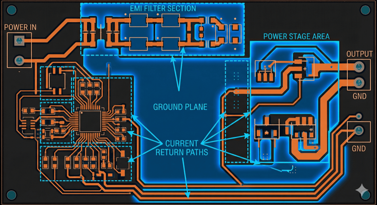
PCB Layout for EMC
Many EMC problems originate from poor PCB layout. Following these guidelines reduces emissions at the source.
Power Stage Layout:
-
Minimize Loop Area:
- Current loops radiate proportionally to area
- Place decoupling caps as close as possible to switches
- Use wide, short traces for high-current paths
- Consider multi-layer stackup with power/ground planes
-
Gate Drive Layout:
- Keep gate drive loops small and away from power stage
- Use twisted pair or close-coupled traces
- Separate gate return from power return
-
Switching Node:
- Minimize copper area at switching node (high dV/dt)
- Add snubbers if ringing is excessive
- Consider shielding if node is large
Signal/Control Layout:
-
Separation:
- Keep control circuits away from power stage
- Use ground plane to provide shielding between sections
- Route sensitive signals away from switching nodes
-
Grounding:
- Use star ground or ground plane
- Don't let high-current return paths cross sensitive areas
- Connect ground plane to chassis at strategic locations
-
Clock/Oscillator:
- Shield crystal oscillators
- Use spread spectrum clocking if available
- Filter clock lines before leaving board
Input/Output:
-
Filter at Board Edge:
- Place EMI filter components at cable entry points
- Don't let filtered and unfiltered traces run parallel
- Use guard traces or ground between input and output
-
Connector Grounding:
- Provide solid ground connection for shielded connectors
- Use 360° shield termination when possible
- Include ground pins adjacent to signal pins
Common Failure Modes and Fixes
When pre-compliance testing reveals problems, here are the most common issues and solutions:
Failure: Conducted Emissions at Switching Frequency Harmonics
Root Cause: Insufficient filtering of switching frequency noise Fixes:
- Add/increase differential mode filter (larger L, larger C)
- Add common mode choke if CM current is significant
- Reduce switching speed (increase gate resistance)
- Use soft switching if topology allows
Failure: Conducted Emissions in 5-30MHz Range
Root Cause: Parasitic ringing, often at power stage Fixes:
- Add RC snubber across switches
- Improve decoupling cap placement
- Add ferrite bead in series with problematic nodes
- Check for and eliminate parasitic inductance
Failure: Radiated Emissions 30-200MHz
Root Cause: Cables acting as antennas, large current loops Fixes:
- Add common mode chokes on cables
- Improve shielding/filtering at cable entry
- Reduce loop area in power stage
- Add enclosure shielding
Failure: Radiated Emissions 200MHz-1GHz
Root Cause: High-speed digital signals, harmonics of fast edges Fixes:
- Slow down unnecessary fast edges
- Filter clock/data lines before cable entry
- Improve enclosure shielding
- Add ferrites on I/O cables
Failure: Radiated Emissions from Display/HMI
Root Cause: Long cables to displays, touch screens Fixes:
- Use shielded cables with filtered connectors
- Add CM chokes near enclosure exit
- Consider fiber optic isolation for extreme cases
Failure: Immunity (ESD, Surge, EFT)
Root Cause: Insufficient protection devices, poor grounding Fixes:
- Add TVS diodes at I/O interfaces
- Improve chassis grounding
- Add protection on all external connections
- Verify ground continuity throughout enclosure
Free Resource: Download our EMI/EMC Design Rulebook — a 15-page practical guide with design rules specifically for power electronics EMC compliance.